薄膜太陽電池市場が2033年に61億米ドルに拡大する見通し
薄膜&フレキシブル太陽電池 2023-2033年
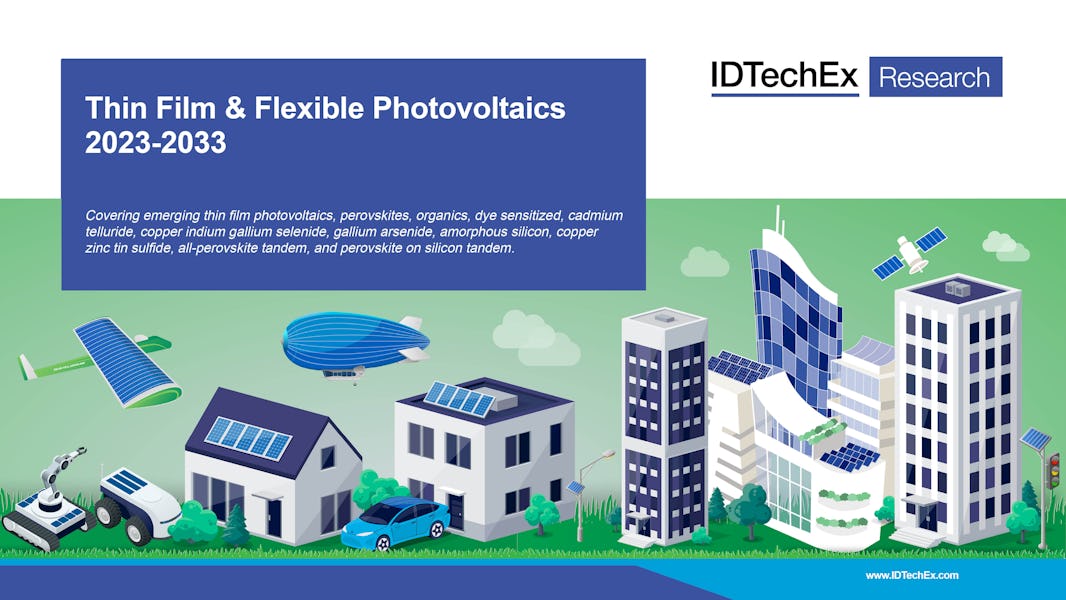
最新の薄膜太陽電池(ペロブスカイト、有機、色素増感、カドミウムテルライド、セレン化銅インジウムガリウム、ガリウムヒ素、アモルファスシリコン、銅-亜鉛-スズ-硫黄、全ペロブスカイトタンデムおよびペロブスカイト型シリコンタンデム)を網羅
製品情報
概要
目次
価格
Related Content
太陽電池技術の未来はシリコンをはるかに超えて「薄膜」と呼ばれる特定のクラスに属する数多くの代替材料に広がっています。これらの材料は、高効率の屋内エナジーハーベスティング、製造の簡略化、従来のシリコン製 PV よりも潜在的な低コストの可能性など、ユニークな利点をもたらします。特に家庭や店舗の電子機器のスマート化が進み、急速に市場が拡大しているモノのインターネット(Internet of Things)機器に電力を供給する役割を期待されています。
「薄膜&フレキシブル太陽電池 2023-2033年」が対象とする主なコンテンツ
(詳細は目次のページでご確認ください):
● 全体概要および結論
● 薄膜PV タイプ別2023年-2033年市場見通し。設置容量、市場シェア、モジュールコスト、予想売上高を網羅。
● 色素増感、有機&ペロブスカイト PV を含む有機/ハイブリッド薄膜 PV の技術と市場機会分析
● カドミウムテルライド、セレン化銅インジウムガリウム、ガリウムヒ素、アモルファスシリコン、銅-亜鉛-スズ-硫黄を含む従来シリコン製 PVの代替的な無機薄膜技術と市場機会分析
● ペロブスカイト型シリコンタンデム PV および全ペロブスカイトタンデム PV の分析。動機とアプリケーション、業界の有力企業情報
● 材料工学および封止剤に加え有機/ハイブリッドとペロブスカイト PV を巡る安定性の課題評価
● 基板、電荷移動、活物質層用の従来および最新材料評価
「薄膜&フレキシブル太陽電池 2023-2033年 」は以下の情報を提供します
技術動向とメーカー分析:
- 薄膜太陽電池の概要と技術的・商用的成熟度評価
- 主要薄膜 PV 技術であるセレン化銅インジウムガリウム(CIGS)、カドミウムテルライド(CdTe)の最新開発状況と市場動向予測
- ペロブスカイト、有機、色素増感、カドミウムテルライド、セレン化銅インジウムガリウム、ガリウムヒ素、アモルファスシリコン、銅-亜鉛-スズ-硫黄の特性比較。業界での導入拡大の適合性評価。
- 異なる薄膜 PV セルデザインのトレンドと考慮すべき妥協点/要因
- 各技術が直面する最大の課題や競争がもっとも激しい部分に関する議論
- 薄膜 PV が既存シリコン PV と同等の役割を果たす、もしくは代替技術となる可能性のあるニッチ用途特定
- 各技術の異なる製造プロセスに対する費用対効果検証
- 最先端 PV 技術のサプライチェーンにおける主なイノベーションの余地特定
市場予測と分析:
- ソーラーファーム、建材一体型 PV 、ワイヤレスエレクトロニクス用途を網羅した10年先市場見通し(数量と売上高)
- 薄膜 PV タイプ別10年先市場見通し
The future of solar technology extends far beyond silicon, with numerous alternative materials that belong to a certain class called 'thin film'. These can deliver several unique advantages such as higher efficiency indoor energy harvesting, simpler manufacturing, and potentially lower costs than conventional silicon PV. A particularly exciting opportunity is their role in powering Internet of Things devices - a rapidly growing market following the increasing smartification of home and retail electronics.
Decarbonization of global energy sources is being catapulted forward as both nations and industries race to achieve net zero, with photovoltaics (PV) already the fastest growing technology. While silicon PV is affordable to consumers and delivers high efficiencies, its application range is limited by its weight, size, and rigidity as well as a complicated manufacturing process. Thin film alternatives present numerous advantages to overcome these limitations and cater to emerging applications such as indoor energy harvesting.
Photovoltaics diversifying into emerging markets
The thin film PV market share has been steady at 5% of annual PV production for the past few years. However, the market is forecast to grow at a CAGR of 10% over the next 10 years. Firstly, there have been improvements in silicon PV alternatives, with efficiencies increasing gradually and manufacturing processes becoming cheaper and more streamlined. Secondly, new applications are being developed that conventional silicon PV is not suitable for due to its rigidity, bulk, and weight. These applications include building integrated PV (BIPV), where the panels are attached to sides of buildings. In many cases, thin film PV panels can be up to 90% lighter than silicon panels and therefore are particularly suitable for applications where weight is an important factor, such as on building façades or weak structures. Some types of thin film PV can be made semi-transparent, which makes them less aesthetically obtrusive and ideally suited to deployment on windows.
Other emerging applications belong to the small self-powered electronics and Internet of Things (IoT) sector, which is expected to grow substantially in the coming years as 'smart' electronics become more prevalent in everyday life. Lightweight thin film minimodules can be used to power such devices and could serve as a cheaper and more long-lasting alternative to batteries or extensive wiring. Many household and retail appliances such as temperature, humidity, motion, and security sensors are likely to become increasingly 'smart' over the next decade and able to transmit data to the cloud to enable greater functionality. This is often referred to as the Internet of Things (IoT) and represents a substantial opportunity for thin film PV.

Emerging thin film photovoltaics can be printed onto lightweight flexible substrates
What will dominate the thin film market?
Currently, the thin film market is dominated by cadmium telluride (CdTe), followed in second place by copper indium gallium selenide (CIGS). CdTe is best known in the USA where it is used for 40% of all utility-scale PV power. Despite concerns over the use of the scarce element tellurium, the CdTe market is expected to keep its position following strong investment and the creation of recovery and recycling initiatives that are at present already operative.
CIGS technology on the other hand has been plagued by commercial failures, with the largest manufacturer having exited the market in June 2022. It is expected that CIGS will be surpassed in the coming years by perovskite PV - a very young and exciting technology that has shown remarkable efficiency gains in just a few years, with record efficiencies already on par with those of silicon PV, a technology with decades of research behind it. Perovskite PV is well-suited to both outdoor high power density applications as well as indoor energy harvesting and powering small electronics. Perovskite PV does not use toxic or rare materials, and the manufacturing is well-suited to scalable solution-based deposition methods. Despite all these benefits of perovskite PV, concerns over long-term durability have raised a lot of questions regarding their imminent commercialization.
Organic PV is another contender in this area and is already commercial on a small scale in both outdoor and indoor applications. Given the short lifespans of organic solar cells, typically 5 years, they are better to suited to powering short-term use electronics rather than large area outdoor energy harvesting that are expected to last > 15 years. For this reason, the application range of organic PV is limited. Another thin film PV technology is dye sensitized solar cells (DSSCs). DSSCs have been studied for decades; however, commercial traction is relatively recent. It is now possible to buy wireless headphones and smart helmets powered by DSSCs. Adidas is working to incorporate DSSCs into their own headphone line in the future. Similarly to organic PV, DSSCs do not have long lifespans and therefore their application range is also limited to short-term use electronics.
Outlook
The thin film PV market is set to grow to US$ 6.1 billion by 2033. This follows significant expansion of cadmium telluride PV into both rooftop and solar farms markets as well as the burgeoning commercialization of perovskite PV. Perovskite PV is being developed for large outdoor installations but is also a very promising technology for indoor energy harvesting and powering small electronic devices and Internet of Things - these are markets that are set to grow rapidly in coming years as 'smart' technology becomes widespread. Along with the growth of these technologies comes substantial innovation and materials opportunities. Solar cells are increasingly being developed on flexible metal foils and plastic films, and their long-term durability requires high quality encapsulation. Optimizing materials to meet emerging applications and consumer demand is a compelling market opportunity.
Key questions answered in this report
- What thin film PV and how can it be used to address climate change?
- What are the competitive existing PV technologies?
- What are the various market segmentations?
- What is the technology readiness level of each thin film PV technology?
- What are the key drivers and hurdles for market growth?
- Where are the key growth opportunities?
- Who are the key players?
- What are the most lucrative innovation opportunities?
- What are the emerging or untapped application areas?
IDTechEx has 10 years of expertise covering printed and flexible electronics, including thin film photovoltaics. Our analysts have closely followed the latest developments in the technology and associated markets, interviewed key players across the supply chain, attended conferences, and delivered consulting projects on the field. This report examines the current status and latest trends in technology performance, supply chain, manufacturing know-how, and application development progress. It also identifies the key challenges, competition and innovation opportunities facing thin film photovoltaics.
IDTechEx のアナリストへのアクセス
すべてのレポート購入者には、専門のアナリストによる最大30分の電話相談が含まれています。
レポートで得られた重要な知見をお客様のビジネス課題に結びつけるお手伝いをいたします。このサービスは、レポート購入後3ヶ月以内にご利用いただく必要があります。
詳細
この調査レポートに関してのご質問は、下記担当までご連絡ください。
アイディーテックエックス株式会社 (IDTechEx日本法人)
電話 03-3216-7209
担当: 村越美和子 m.murakoshi@idtechex.com
| 1. | EXECUTIVE SUMMARY |
| 1.1. | Current landscape of solar PV |
| 1.2. | Could the thin film market share increase? |
| 1.3. | Thin film PV technologies covered in this report (I) |
| 1.4. | Motivation for thin film solar cells |
| 1.5. | Thin film PV technologies covered in this report |
| 1.6. | Typical commercial efficiencies of existing PV technologies |
| 1.7. | Photovoltaics technology readiness status |
| 1.8. | Commercial opportunity for PV technologies |
| 1.9. | Comparing thin film technologies (i) |
| 1.10. | Comparing thin film technologies (ii) |
| 1.11. | CdTe PV suffers from raw material concerns |
| 1.12. | Key CIGS player exited the market in June 2022 |
| 1.13. | The future of GaAs PV? |
| 1.14. | Amorphous silicon PV experiencing market decline |
| 1.15. | Technological transition improves organic PV efficiency and stability |
| 1.16. | Readiness of organic PV materials and opportunities |
| 1.17. | Perovskite PV - rapid efficiency growth |
| 1.18. | Drivers for perovskite PV |
| 1.19. | Comparison of thin film deposition methods |
| 1.20. | Thin film PV industry adoption of deposition methods |
| 1.21. | Key takeaways (i) |
| 1.22. | Key takeaways (ii) |
| 1.23. | Key takeaways (iii) |
| 1.24. | Thin film PV annual revenue |
| 2. | INTRODUCTION |
| 2.1. | Solar energy is the fastest growing energy source |
| 2.2. | Current landscape of solar PV |
| 2.3. | Motivation for thin film solar cells |
| 2.4. | Thin film PV technologies covered in this report (i) |
| 2.5. | Thin film PV technologies covered in this report (ii) |
| 2.6. | Could the thin film market share increase? |
| 2.7. | Typical commercial efficiencies of existing PV technologies |
| 2.8. | Comparing thin film technologies (i) |
| 2.9. | Comparing thin film technologies (ii) |
| 2.10. | Photovoltaics technology status |
| 2.11. | Typical cost of PV technologies |
| 2.12. | Silicon processing is costly and time intensive |
| 2.13. | Thin film PV benefits from greater vertical integration |
| 2.14. | How does a thin film solar cell work? |
| 2.15. | Key solar cell performance metrics |
| 2.16. | Breakdown of following chapters |
| 3. | MARKET FORECASTS |
| 3.1. | Forecasting methodology |
| 3.2. | Forecasting module costs |
| 3.3. | Total installed PV capacity forecast |
| 3.4. | Thin film PV annual production forecast |
| 3.5. | Thin film annual revenue |
| 3.6. | Thin film annual revenue (excluding CdTe) |
| 3.7. | Module costs |
| 3.8. | Cumulative installed solar farm capacity |
| 3.9. | Annual surface area production - solar farms |
| 3.10. | Solar farm annual revenue |
| 3.11. | Solar farm annual revenue (excluding CdTe) |
| 3.12. | Cumulative installed BIPV capacity |
| 3.13. | Annual surface area production - BIPV |
| 3.14. | BIPV annual revenue |
| 3.15. | PV module costs for wireless electronics |
| 3.16. | Production forecast for PV-powered wireless electronics |
| 3.17. | Annual revenue for PV in wireless electronics |
| 4. | EMERGING THIN FILM PHOTOVOLTAICS |
| 4.1. | Overview |
| 4.1.1. | Introduction to emerging thin film PV |
| 4.1.2. | Emerging thin film PV technology status |
| 4.2. | Dye Sensitised Photovoltaics |
| 4.2.1. | Introduction to dye sensitized solar cells |
| 4.2.2. | How does a DSSC work? |
| 4.2.3. | Carbon more practical than platinum as counter electrode |
| 4.2.4. | Opportunities to enhance DSSC electrolyte |
| 4.2.5. | Emerging alternatives to electrolyte solution for DSSC |
| 4.2.6. | Exeger: Utilizing DSSC to harvest energy for consumer goods |
| 4.2.7. | Value propositions of DSSC PV for indoor energy harvesting of consumer devices |
| 4.2.8. | Exeger's partnerships show promising future of DSSCs |
| 4.2.9. | DSSC-powered AR/VR headsets? |
| 4.2.10. | Solaronix - DSSC materials provider turning to perovskites |
| 4.2.11. | Innovation opportunities within DSSCs |
| 4.2.12. | Porter's Five Forces: DSSC PV Market |
| 4.2.13. | SWOT: Dye sensitised PV |
| 4.2.14. | Key Takeaways: DSSCs |
| 4.3. | Organic Photovoltaics |
| 4.3.1. | Introduction to organic PV |
| 4.3.2. | OPV: How does it work? |
| 4.3.3. | Advantages of organic PV relative to conventional silicon PV(i) |
| 4.3.4. | Advantages of organic PV relative to conventional silicon PV (ii) |
| 4.3.5. | Significant lag between lab and industry |
| 4.3.6. | Key players in the OPV industry |
| 4.3.7. | Porter's Five Forces: Organic PV Market |
| 4.3.8. | SWOT: Organic PV |
| 4.4. | Organic PV Materials Opportunities |
| 4.4.1. | Types of organic PV materials |
| 4.4.2. | Organic materials: Molecules vs polymers |
| 4.4.3. | Technological transition improves organic PV efficiency and stability |
| 4.4.4. | Benefits of non-fullerene acceptors in OPV (i) |
| 4.4.5. | Benefits of non-fullerene acceptors in OPV (ii) |
| 4.4.6. | Examples of non-fullerene acceptors |
| 4.4.7. | Tuneable band gaps make OPV well-suited to niche applications |
| 4.4.8. | Brilliant Matters producing speciality organic inks |
| 4.4.9. | Benefits of Brilliant Matters' unique polymerization methodology |
| 4.4.10. | Raynergy Tek targeting high efficiency OPV |
| 4.4.11. | OPV materials opportunities |
| 4.4.12. | Readiness of organic PV materials |
| 4.4.13. | Key takeaways: Organic PV |
| 4.5. | Perovskite Photovoltaics |
| 4.5.1. | What is perovskite PV? |
| 4.5.2. | Perovskite PV - A high achiever |
| 4.5.3. | Perovskite solar cell evolution |
| 4.5.4. | n-i-p vs p-i-n configurations |
| 4.5.5. | Simple structures for scalable perovskite PV |
| 4.5.6. | Emerging research topics in perovskite PV |
| 4.5.7. | Perovskite research begins to plateau |
| 4.5.8. | Perovskite PV incentivisation |
| 4.5.9. | Has perovskite PV lived up to early expectations? |
| 4.5.10. | Perovskite PV could be low-cost alternative to GaAs |
| 4.5.11. | Perovskites can save time, money, and energy relative to silicon PV |
| 4.5.12. | Perovskite PV challenges |
| 4.5.13. | Stability poses a challenge to commercialisation |
| 4.5.14. | Extrinsic degradation |
| 4.5.15. | Intrinsic degradation mechanisms |
| 4.5.16. | Material engineering can improve stability but compromise optical properties |
| 4.5.17. | Commercialisation of perovskite PV underway |
| 4.5.18. | Porter's Five Forces: Thin film perovskite PV market |
| 4.5.19. | SWOT analysis of thin film perovskite PV |
| 4.6. | Perovskite PV Materials Opportunities |
| 4.6.1. | Perovskite Material Components |
| 4.6.2. | Are lead concerns justified? |
| 4.6.3. | Public perception vs reality of lead |
| 4.6.4. | Material composition influences light absorption |
| 4.6.5. | Perovskite active layer materials - a commoditised market |
| 4.6.6. | High demand for low cost transport layers |
| 4.6.7. | Organic charge transport layers have high complexity |
| 4.6.8. | SFX - An alternative to Spiro as a hole transport layer? |
| 4.6.9. | Charge transport layer can limit cell efficiency |
| 4.6.10. | Inorganic charge transport layers are a simpler alternative to organic materials |
| 4.6.11. | Key takeaways: Perovskite PV |
| 4.7. | Applications for Emerging PV |
| 4.7.1. | Introduction: Applications for emerging PV |
| 4.7.2. | Current state of application development |
| 4.7.3. | Meeting application requirements - existing silicon vs thin film perovskite |
| 4.7.4. | Thin film PV for indoor energy harvesting |
| 4.7.5. | Thin film PV targets emerging IoT Applications |
| 4.7.6. | Perovskite PV could be cost-effective alternative for wireless energy harvesting |
| 4.7.7. | Solar powered smart packaging |
| 4.7.8. | Epishine has largest IP portfolio on OPV |
| 4.7.9. | Epishine is leading the way in solar powered IoT |
| 4.7.10. | Epishine considering entering perovskite PV market |
| 4.7.11. | Ribes Tech - OPV developer making customizable OPV modules |
| 4.7.12. | Ribes Tech targeting IoT market |
| 4.7.13. | Dracula Technologies aiming for low-cost small OPV modules |
| 4.7.14. | Dracula Tech intending >5 million piece production capacity by 2024 (i) |
| 4.7.15. | Dracula Tech intending >5 million piece production capacity by 2024 (ii) |
| 4.7.16. | infinityPV developing organic PV powered portable chargers |
| 4.7.17. | Saule Technologies: Perovskite PV developer for indoor electronics |
| 4.7.18. | Saule Technologies developing perovskite PV powered electronic shelf labels |
| 4.7.19. | Perovskite PV for vertical building integration |
| 4.7.20. | Tuneable bandgaps make thin film PV well suited to niche applications |
| 4.7.21. | Ubiquitous Energy developing organic PV glass |
| 4.7.22. | Could thin film PV be used to power cars? |
| 4.7.23. | Perovskite PV for conventional applications |
| 4.7.24. | Key takeways: Applications |
| 4.8. | Scalable Deposition Methods |
| 4.8.1. | Deposition techniques for scalable processing |
| 4.8.2. | Sputtering for high purity deposition |
| 4.8.3. | AACVD is an emerging solution-based vacuum approach |
| 4.8.4. | Inkjet printing for high spatial resolution |
| 4.8.5. | Blade coating is cheap but inconsistent |
| 4.8.6. | Slot-die coating is promising for industry |
| 4.8.7. | Spray coating - rapid but wasteful |
| 4.8.8. | Poor spatial resolution wastes material |
| 4.8.9. | Comparison of deposition methods |
| 4.8.10. | How to decide on thin film deposition methods? |
| 4.8.11. | Towards roll-to-roll printing |
| 4.8.12. | Novel perovskite deposition technique by Creaphys/MBraun |
| 4.8.13. | Thin film PV industry adoption of deposition methods |
| 4.8.14. | Summary of Deposition Methods |
| 4.9. | Substrates and Encapsulation Materials |
| 4.9.1. | Introduction: Substrates and encapsulation for thin film PV |
| 4.9.2. | Substrate choices: Conventional and emerging |
| 4.9.3. | Limitations of rigid glass substrates |
| 4.9.4. | Alternatives to rigid glass |
| 4.9.5. | What is ultra-thin flexible glass? |
| 4.9.6. | Ultra-thin glass improves flexibility |
| 4.9.7. | Encapsulation advantages of ultra-thin flexible glass |
| 4.9.8. | Corning Willow flexible glass: Market leader |
| 4.9.9. | Schott Solar flexible glass for aerospace |
| 4.9.10. | Flexible glass substrates: Advantages and disadvantages |
| 4.9.11. | Plastic substrates - cheap and flexible |
| 4.9.12. | Barrier layer requirement increases cost of plastic substrates |
| 4.9.13. | Why use metal foil substrates? |
| 4.9.14. | Substrate surface roughness impacts cell performance |
| 4.9.15. | Substrate material supply opportunities |
| 4.9.16. | Substrate cost comparison |
| 4.9.17. | Benchmarking substrate materials |
| 4.9.18. | How to choose a substrate |
| 4.9.19. | Glass-glass encapsulation to prevent extrinsic degradation |
| 4.9.20. | Comparison of common polymer encapsulant materials |
| 4.9.21. | Thin film encapsulation |
| 4.9.22. | Al2O3 is an upcoming thin film encapsulant |
| 4.9.23. | Ergis providing flexible barrier films with exceptionally low WVTR |
| 4.9.24. | Commercial flexible encapsulation |
| 4.9.25. | Opportunities within substrates and encapsulation |
| 4.9.26. | Key takeaways: substrates and encapsulation |
| 5. | INORGANIC ALTERNATIVES TO SILICON PV |
| 5.1. | Overview |
| 5.1.1. | Introduction: Inorganic alternatives to silicon |
| 5.1.2. | Inorganic PV comparisons |
| 5.1.3. | Readiness levels of inorganic alternatives to silicon PV |
| 5.1.4. | Summary of inorganic alternatives to silicon PV |
| 5.2. | Cadmium Telluride (CdTe) |
| 5.2.1. | Introduction to CdTe PV: The second most common PV technology |
| 5.2.2. | CdTe Photovoltaics: How does it work? |
| 5.2.3. | New CdTe cell structure increases efficiency |
| 5.2.4. | Why CdTe PV? |
| 5.2.5. | CdTe market share - has it plateaued? |
| 5.2.6. | CdTe PV plagued by toxicity concerns |
| 5.2.7. | CdTe PV suffers from raw material concerns |
| 5.2.8. | Does CdTe face a production limit? |
| 5.2.9. | First Solar's monopoly - room for entry? |
| 5.2.10. | The unexplored rooftop market |
| 5.2.11. | Can Toledo Solar crack emerging markets? |
| 5.2.12. | Alternative absorber materials |
| 5.2.13. | Innovation opportunities for CdTe PV |
| 5.2.14. | SWOT: CdTe PV |
| 5.2.15. | Porter's Five Forces: CdTe PV Market |
| 5.2.16. | Key takeaways: CdTe PV |
| 5.3. | Copper Indium Gallium Selenide (CIGS) |
| 5.3.1. | Introduction to CIGS PV |
| 5.3.2. | CIGS PV: How does it work? |
| 5.3.3. | Value propositions of CIGS PV |
| 5.3.4. | Why has CIGS PV struggled to gain ground? |
| 5.3.5. | Key player exited the market in June 2022 |
| 5.3.6. | Aesthetics are important for BIPV |
| 5.3.7. | Could flexible CIGS solar cells take off? |
| 5.3.8. | Midsummer making flexible cadmium-free CIGS solar cells |
| 5.3.9. | Midsummer targeting rooftop market |
| 5.3.10. | Midsummer attempting expansion into aerospace |
| 5.3.11. | Transition toward cadmium-free cells |
| 5.3.12. | The search for simple low cost deposition |
| 5.3.13. | CIGS PV innovation opportunities |
| 5.3.14. | SWOT: CIGS PV |
| 5.3.15. | Porter's Five Forces: CIGS PV Market |
| 5.3.16. | Key takeaways: CIGS PV |
| 5.4. | Gallium Arsenide |
| 5.4.1. | Introduction to GaAs PV |
| 5.4.2. | GaAs PV: How does it work? |
| 5.4.3. | Multi-junction GaAs solar cells |
| 5.4.4. | Properties of GaAs PV |
| 5.4.5. | The future of GaAs PV? |
| 5.4.6. | Key player Alta Devices has shut down |
| 5.4.7. | Slow manufacturing is an issue for GaAs |
| 5.4.8. | NREL working on inexpensive manufacturing |
| 5.4.9. | Solar cars - an Earth application of GaAs PV? |
| 5.4.10. | GaAs PV innovation opportunities |
| 5.4.11. | SWOT: GaAs PV |
| 5.4.12. | Porter's Five Forces: GaAs PV Market |
| 5.4.13. | Key takeaways: GaAs PV |
| 5.5. | Amorphous Silicon |
| 5.5.1. | Amorphous silicon: What is it? |
| 5.5.2. | Amorphous silicon PV: How does it work? |
| 5.5.3. | Deposition of amorphous silicon |
| 5.5.4. | Onyx Solar producing PV glass with amorphous silicon |
| 5.5.5. | Amorphous silicon PV experiencing market decline |
| 5.5.6. | Conventional silicon PV using amorphous silicon |
| 5.5.7. | Photovoltaic thermal collectors: a potential application of amorphous silicon? |
| 5.5.8. | Does amorphous silicon PV have a future? |
| 5.5.9. | Amorphous silicon PV innovation opportunities |
| 5.5.10. | Porter's Five Forces: a-Si PV Market |
| 5.5.11. | SWOT: Amorphous silicon PV |
| 5.5.12. | Key takeaways: Amorphous silicon PV |
| 5.6. | Copper Zinc Tin Sulfide (CZTS) |
| 5.6.1. | What is CZTS photovoltaics? |
| 5.6.2. | CZTS PV: How does it work? |
| 5.6.3. | Cadmium-free buffer layers |
| 5.6.4. | Crystalsol commercialising CZTS PV |
| 5.6.5. | CZTS as a hole-transport layer in perovskite solar cells |
| 5.6.6. | Solution processing of CZTS |
| 5.6.7. | CZTS PV innovation opportunities |
| 5.6.8. | Porter's Five Forces: CZTS PV Market |
| 5.6.9. | SWOT: CZTS PV |
| 5.6.10. | Key Takeaways: CZTS PV |
| 6. | TANDEM PHOTOVOLTAICS |
| 6.1. | Overview |
| 6.1.1. | Introduction to tandem photovoltaics |
| 6.1.2. | Single junction vs tandem solar cells |
| 6.1.3. | Tandem solar cells to surpass theoretical efficiency limits of a single junction |
| 6.2. | Perovskite on Silicon Tandem |
| 6.2.1. | Perovskite on silicon tandem advantages |
| 6.2.2. | Tandem cell configurations |
| 6.2.3. | Perovskite on silicon tandem cell challenges |
| 6.2.4. | Perovskite on silicon tandem process flow |
| 6.2.5. | Silicon-perovskite tandem cost breakdown |
| 6.2.6. | Oxford PV: Major player in perovskite on silicon tandem PV |
| 6.2.7. | Business model of Oxford PV |
| 6.2.8. | Oxford PV is entering an unestablished market |
| 6.2.9. | CubicPV: Early stage perovskite on silicon developer |
| 6.2.10. | CubicPV's Direct Wafer® Method |
| 6.2.11. | Cubic PV delays timeline for tandem perovskite-on-silicon PV |
| 6.2.12. | Summary of key players (perovskite on silicon tandem) |
| 6.2.13. | Perovskite on silicon tandem PV roadmap |
| 6.2.14. | Porter's Five Forces: perovskite on silicon tandem PV market |
| 6.2.15. | SWOT analysis of perovskite on silicon tandem PV |
| 6.2.16. | Key takeaways: perovskite on silicon tandem |
| 6.3. | All-Perovskite Tandem |
| 6.3.1. | Current status of all-perovskite tandem solar cells |
| 6.3.2. | Bottom cell poses key challenge |
| 6.3.3. | Tin-based perovskites react with HTL |
| 6.3.4. | Emergence of HTL-free perovskite cells |
| 6.3.5. | Carbon-based HTL-free perovskite cells |
| 6.3.6. | Do HTL-free cells have a future? |
| 6.3.7. | Swift Solar: Developing all-perovskite tandem cells |
| 6.3.8. | Swift Solar's all-perovskite approach |
| 6.3.9. | Swift Solar all-perovskite tandem PV for electric cars |
| 6.3.10. | Non-solution deposition techniques could benefit all-perovskite tandem |
| 6.3.11. | Porter's Five Forces: all-perovskite tandem PV market |
| 6.3.12. | SWOT analysis of all-perovskite tandem PV |
| 6.3.13. | Key takeaways: all-perovskite tandem |
| 6.4. | Emerging Tandem Applications |
| 6.4.1. | Solar cell structures for different applications |
| 6.4.2. | Perovskite on silicon tandem PV coming to rooftops soon |
| 6.4.3. | Could tandem PV be integrated into windows? |
| 6.4.4. | Aesthetics may trump efficiency |
| 6.4.5. | Could all-perovskite tandem deliver solar powered vehicles? |
| 6.4.6. | Lightyear: Long range solar electric vehicle |
| 6.4.7. | Key takeaways: tandem PV applications |
| 7. | COMPANY PROFILES |
| 7.1. | Asca |
| 7.2. | Avancis |
| 7.3. | Brilliant Matters |
| 7.4. | Corning |
| 7.5. | Crystalsol |
| 7.6. | CubicPV |
| 7.7. | Dracula Technologies |
| 7.8. | EMC |
| 7.9. | Epishine |
| 7.10. | Exeger |
| 7.11. | GCL |
| 7.12. | Greatcell Solar |
| 7.13. | Heliatek |
| 7.14. | Microquanta Semiconductor |
| 7.15. | Midsummer |
| 7.16. | Onyx Solar |
| 7.17. | Opteria |
| 7.18. | Oxford PV |
| 7.19. | infinityPV |
| 7.20. | Raynergy Tek |
| 7.21. | Ribes Tech |
| 7.22. | Saule Technologies |
| 7.23. | Schott |
| 7.24. | Solaronix |
| 7.25. | Sunew |
| 7.26. | Swift Solar |
| 7.27. | Toledo Solar |
価格および注文方法
薄膜&フレキシブル太陽電池 2023-2033年
£€$¥元
電子版_PDF(ユーザー 1-5名)
£5,650.00
電子版_PDF(ユーザー 6-10名)
£8,050.00
電子版_PDFおよびハードコピー1部(ユーザー 1-5名)
£6,450.00
電子版_PDFおよびハードコピー1部(ユーザー 6-10名)
£8,850.00
電子版_PDF(ユーザー 1-5名)
€6,400.00
電子版_PDF(ユーザー 6-10名)
€9,100.00
電子版_PDFおよびハードコピー1部(ユーザー 1-5名)
€7,310.00
電子版_PDFおよびハードコピー1部(ユーザー 6-10名)
€10,010.00
電子版_PDF(ユーザー 1-5名)
$7,000.00
電子版_PDF(ユーザー 6-10名)
$10,000.00
電子版_PDFおよびハードコピー1部(ユーザー 1-5名)
$7,975.00
電子版_PDFおよびハードコピー1部(ユーザー 6-10名)
$10,975.00
電子版_PDF(ユーザー 1-5名)
¥900,000
電子版_PDF(ユーザー 6-10名)
¥1,260,000
電子版_PDFおよびハードコピー1部(ユーザー 1-5名)
¥1,020,000
電子版_PDFおよびハードコピー1部(ユーザー 6-10名)
¥1,380,000
電子版_PDF(ユーザー 1-5名)
元50,000.00
電子版_PDF(ユーザー 6-10名)
元72,000.00
電子版_PDFおよびハードコピー1部(ユーザー 1-5名)
元58,000.00
電子版_PDFおよびハードコピー1部(ユーザー 6-10名)
元80,000.00
Click here to enquire about additional licenses.
If you are a reseller/distributor please contact us before ordering.
お問合せ、見積および請求書が必要な方はm.murakoshi@idtechex.com までご連絡ください。
レポート概要
| スライド | 329 |
|---|---|
| フォーキャスト | 2033 |
| ISBN | 9781915514158 |
コンテンツのプレビュー
 Webinar Slides - EOY 2022 Webinar Slides - EOY 2022
|
|
Webinar Slides
|
|
Sample pages
|
|
|